The prerequisite that the reader should come with is study of 5th chapter of the “Computer Architecture” book by “Morris Mano“. For your help I have added an e-book for the same here.
However, those who are well aware of the basic architecture can directly jump to study the basic Verilog Code provided. The complete architecture has been made using the Xilinx software and the implementation has been implemented on the target device: xc5vlx110t-3ff1136. For clarity, I provide a breif description herewith,
Load all the verilog codes that you download in a single project on Xilinx.
1. CU.V is the main black box or you can say your basic computer that includes all the hardware and wirings inside it.
2. MEM.V is the ROM memory being used for this example. It has a capacity to store 256words of 16 bits each. I could have used 2 separate memories for instructions and data but being stuck with making a ‘basic’ example I left out the same. You are, although, eligible to do the same 😉 You may frown on me for not choosing a block RAM. Don’t worry, soon I’ll post an example including the same.
3. SIGNALS.V is the signal generator module that provides all the required timing signals for the computer to work with. It’s basically the T0, T1, T2… timing signals which are used to schedule the fetch and execute instructions through the control block.
4. REGISTER.V is a basic module describing the registers of the architecture. Anyone with hands on Verilog can hold it with ease.
5. ALU.V is the block that describes the Arithmetic Logic Unit of the system. This module takes the signal from the control block and performs all the operations related with the Accumulator (AC) and the carry flip-flop (E).
6. FF.V implements the flip-flop model. I have only used the E flip-flop. Anyone who is more excited can use this module to extend the complete design by including the parity, sign and other flip-flops to this basic architectue design.
7. OPCODE.V is used to reduce the complexity involved with decoding the Instruction register’s (IR) higher bits. This decoder is used to decode the 12,13 and 14 bits of the IR code.
8. CTRL.V is the heart of the design. Yeah! you guessed right, this module describes all the timing sequences associated with computer.
So, with some info about the modules now you are all set to dig in for more. Click here to fork the Xilinx project.
An RTL Schematic of the project is here: 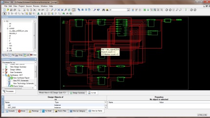
More into the inside:
In the downloaded architecture provision has only been made to work with the memory reference and the register reference instructions (you can get the list from the book). Their is no provision to work with the input/output instructions and the interrupt cycle.
I have also included a text file called “t.txt” with an example program that can be burned into the ROM. You can write your own program for further testing purpose using the hexadecimal coding provided in the book. (I’ll soon post a C++ program to help you with it). The description of the testing program is:
Hexadecimal Code Meaning
200a Load content from memory to AC. It loads the data from address ‘a’ to AC.
100b ADD to AC the content stored at address ‘b’ from ROM.
300c Store the content of AC at address ‘c’ in ROM.
200c Load the content from ROM address ‘c’ in AC.
7020 Increment AC
7400 Clear E
7080 Circulate AC right
7100 Complement E
7040 Circulate AC left
0000 Do Nothing
0f0f The data stored at the ROM address ‘a’
f102 The data stored at the ROM address ‘b’
Basically I attempted to test some memory reference and register reference instructions using this code. You can go with your own testing skills.
For any queries or any doubts feel free to contact me.

hey, it’s so good, i used it for my computer architecture project
but there was some mistakes you had, and it killed me to fix them, but i finally fixed some, if you want the changed files, email me : favarjooy86@gmail.com
the problems were :
1- there was no output in the controller module to pc_idat.
the pc_idate input of the pc module is wired to nothing.
2- the pc_odat can’t be controlled by the “ISZ, BUN, SZA, ..” and every assembly instructions which should actually change the value of pc, it just increase and increase untli the end of the memory, i fixed that by including some lines of program that makes the pc_odat be controllable.
3- one of the most confusing : the T[4] signal introduced in the “M.Mano Computer Architecture” is not the dec_signal[4] in the program, it’s actually dec_signal[5], WOW, I don’t know how did I found that. God. and it’s not just T[4], T[2] is like the same. maybe some other T too 😀
at the last i had to change the cu.v for making up some other wires and create needed connections.
But man that was awesome. Thank you very much, I could never do that in just 2-days that I had.
Hey good to hear that it created some problem to you. I wanted someone to review this whole framework but no one was interested. I know some mistakes were there but couldn’t find them out. It was a side summer project for me too when I was a sophomore. It gave me some confidence to take on a big one – JPEG 2000 architecture. I’m still to post it here.
I’ll soon move the files over to GIT for people to fork. Then it would be easy for you to check in your corrections. And what took 2 days for you took whole 2 weeks for me, but it was worth it. I’m glad it helped you.
Did you try to include keyboard/mouse interface as well?
hey,
cant wait for the big JPEG 😀
and…, no i didn’t use interruption, the project doesnt need it.
Use the link https://github.com/gmish27/CPUonFPGA to fork the project with your corrections.
oh, github doesn’t work in my country 😐 or maybe my poor internet connection doesnt support it, anyway i coudn’t use it. it doesnt fork, i tried but it’s not working… if it’s necessary email is much easier for me, i can send it to you by email.. sorry for that
Click Here Very nice post. I just stumbled upon your weblog and wanted to say that I have truly enjoyed surfing around your blog posts. In any case I will be subscribing to your rss feed and I hope you write again very soon!
I like the valuable info you provide in your articles. I will bookmark your blog and check again here regularly. I am quite certain I will learn plenty of new stuff right here! Good luck for the next!
Hey, thank you for your appreciation (no_name). Yeah! I’ll surely try to come up with some more good modules and ideas to play with. Moreover, if you have some topics to work on then you can tell me about it as well. Maybe, it turns out into another topic on this blog 😉