


Software apps and online services | ||||||
 |
| |||||
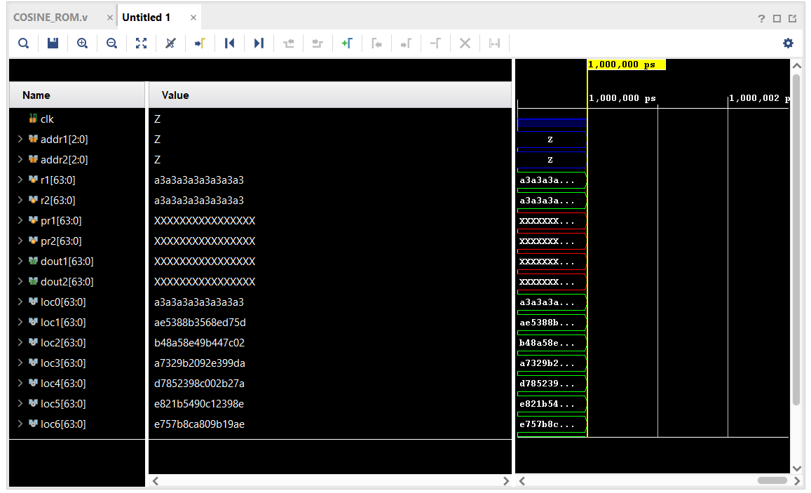
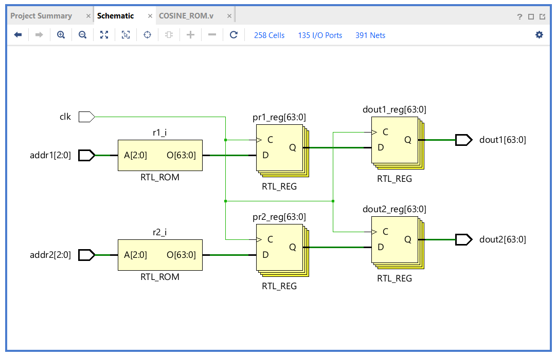
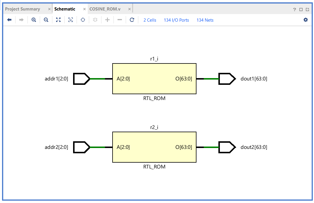
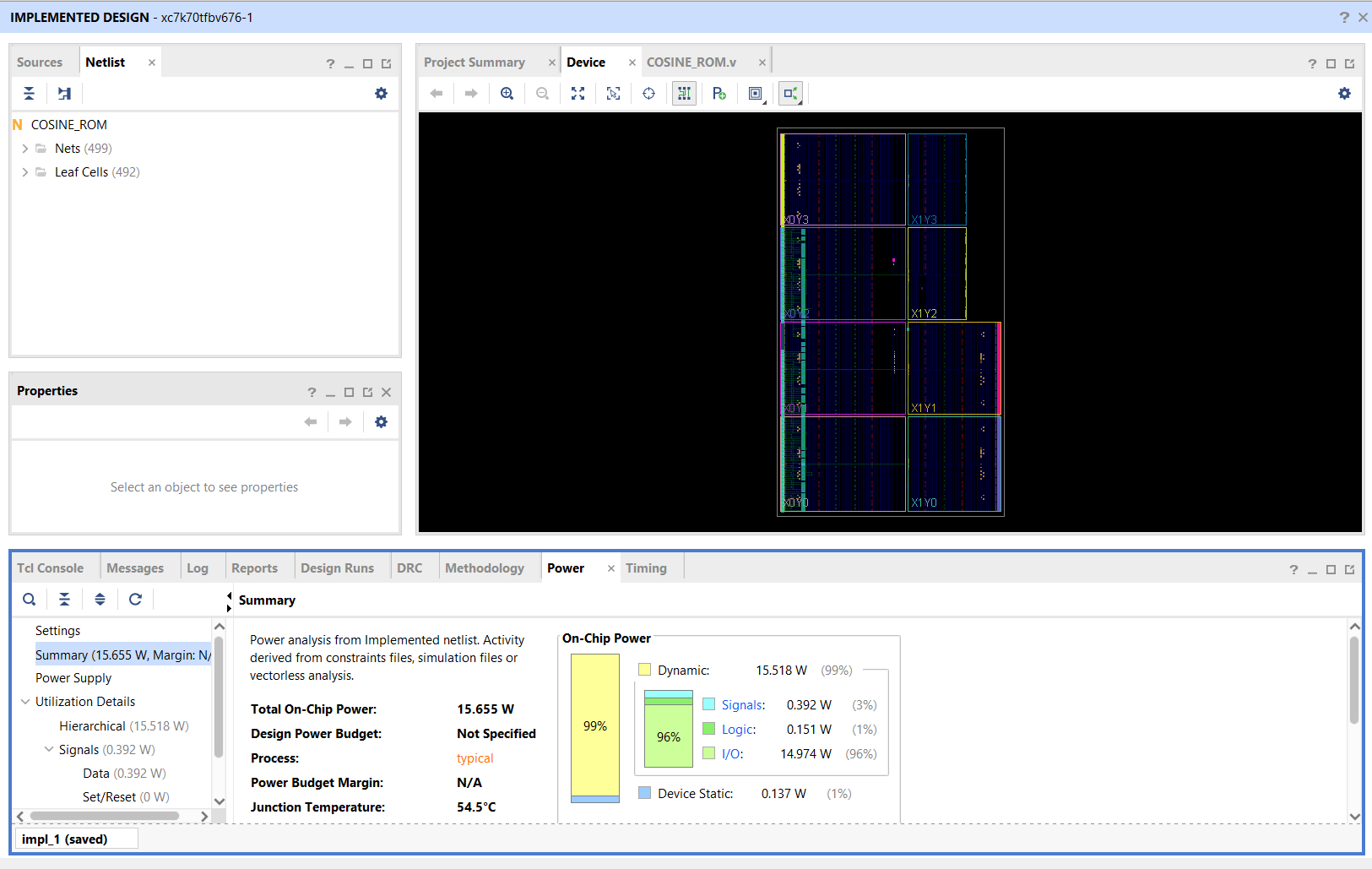
The Dual Address Data Read Only Memory helps in parallel transfer of data. For this, dual address and dual output of data are the main design constraints required. Furthermore, there also a need exists of clock in order to achieve synchronous pipelining (Fetch->Decode->Execute->Write). The number of bits in address bus (i.e. n) results the number of locations in ROM with the exponential of two i.e. 2^n and the data width is 64 bits. Hence, the ROM content the data of 8x64 bits in a unique architectural block.
In DCTQ implementation, the cosine transform coefficient from the block of data as well as cosine terms along its transpose is computed. For this, the value realization is done by using two separate address ROM in which one stores cosine (C) and the other stores its transpose (C^T). Since DCTQ requires both cosine and its transpose simultaneously for performing algorithm, we need dual data address rather than single address. Coming to the need of accuracy, the cosine and its transpose magnitude is made twice during storage and its coefficient is reduced by two, so that it can possess neutrality. Since the output data get delayed by two clock cycles, we also use two stage pipelining to match the pace so that the desired constraints can be achieved at the output.


Comments