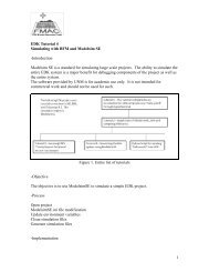
Tutorial 11 ChipscopePro, ISE 10.1 and Xilinx Simulator ... - Cosmiac
Tutorial 11 ChipscopePro, ISE 10.1 and Xilinx Simulator ... - Cosmiac
Tutorial 11 ChipscopePro, ISE 10.1 and Xilinx Simulator ... - Cosmiac

You also want an ePaper? Increase the reach of your titles
YUMPU automatically turns print PDFs into web optimized ePapers that Google loves.
<strong>Tutorial</strong> <strong>11</strong><br />
<strong>ChipscopePro</strong>, <strong>ISE</strong> <strong>10.1</strong> <strong>and</strong> <strong>Xilinx</strong> <strong>Simulator</strong> on the<br />
Digilent Spartan-3E board<br />
Introduction<br />
This lab will be an introduction on how to use ChipScope for the verification of the designs done on<br />
FPGAs. ChipScope Pro <strong>10.1</strong> is the tool provided by <strong>Xilinx</strong> for this purpose. The board will be a<br />
Digilent Spartan-3E starter kit.<br />
Objective<br />
The objective is to verify the functioning of a simple counter implementation using ChipScope. The<br />
counter implemented here is a 4-bit counter operated at five different frequencies. The aim is not to<br />
implement complex digital designs but to show the user a method to integrate ChipScope into an<br />
existing design in order to verify its operation in a simple <strong>and</strong> efficient manner. ChipScope is a virtual<br />
logic analyzer.<br />
Prerequisites<br />
• Basic knowledge about digital design <strong>and</strong> FPGAs.<br />
• Acquaintance with <strong>Xilinx</strong> <strong>ISE</strong> <strong>10.1</strong> <strong>and</strong> <strong>Xilinx</strong> <strong>Simulator</strong> tools.<br />
• ChipScope is not included in <strong>ISE</strong> but is a program available through the <strong>Xilinx</strong> university<br />
program.<br />
Application<br />
This document is used by students, who are learning FPGA design <strong>and</strong> verification.<br />
Design Overview<br />
4-bit counter implemented at five different frequencies using the system clock running at 50 Mhz. The<br />
five frequencies are<br />
50 Mhz<br />
, 50 Mhz<br />
, 50 Mhz<br />
, 50 Mhz<br />
, 50 Mhz<br />
, (the frequencies are<br />
2 3<br />
2 23<br />
2 24<br />
chosen to make the counter action visible through the LEDs, except for the highest frequency which is<br />
2 25<br />
2 26
solely to verify the design in the <strong>ISE</strong> <strong>Simulator</strong>).<br />
The frequencies are controlled using input signal FREQUENCY connected to three of the available<br />
four sliding switches (SW1, SW2 & SW3).<br />
The output of the 4-bit counter is connected to four of the available seven LEDs (LD0, LD1, LD2,<br />
LD3).<br />
An asynchronous reset is also provided to the design which is connected to one of the sliding switches<br />
(SW0).<br />
Process<br />
1. Complete the counter design to implement functionality as explained (provided).<br />
2. Verify inputs <strong>and</strong> outputs with test bench waveform (provided).<br />
3. Integrate the ChipScope into the counter design (explained in detail in the Implementation<br />
section).<br />
4. Analyze the design using ChipScope (also explained in detailed in the next section).<br />
Implementation<br />
1. Right click on the top module of the design intended for verification or debugging, <strong>and</strong> select<br />
new source. Then select ChipScope Definition <strong>and</strong> Connection File as shown below.<br />
Figure 1: ChipScope Module Selection
2. Then give an appropriate name for the file name. Press next <strong>and</strong> select the hierarchy level at<br />
which the analysis is intended to be performed <strong>and</strong> then press next <strong>and</strong> then do finish.<br />
Figure 2: Hierarchy Selection<br />
3. The first two steps will cause a new file (with file name as given) to be created in the source<br />
window under the project hierarchy as shown below.<br />
Figure 3: ChipScope Module Location
4. Double click on this new source file which cause the below window to pop up. Keep the default<br />
settings with Use SRLs <strong>and</strong> Use RPMs as checked.<br />
This will enable the tool to use Shift Register LUTs instead of flip flops <strong>and</strong> multiplexers<br />
thereby effectively reducing the size <strong>and</strong> improving the performance of the core generator.<br />
RPMs contain RLOC constraints which define the order <strong>and</strong> structure of the underlying design<br />
primitives. Use of RPMs will enable the tool to use relationally placed macros (like FMAP,<br />
HMAP, ROM, RAM, etc) allowing logic blocks to be placed relative to increase speed <strong>and</strong> use<br />
die resources efficiently substituting hard macros with an equivalent that can be simulated<br />
directly which again increases the core performance.<br />
Figure 4: SRL <strong>and</strong> RPMs<br />
5. Press next <strong>and</strong> again leave the default conditions i.e., keep the Disable JTAG Clock BUFG<br />
Insertion box unchecked.<br />
Disabling JTAG clock will cause the implementation tool to route the JTAG clock using normal<br />
routing resources instead of global clock routing resources. This might affect the high speed<br />
clock signals. So, unless the global resources are very scarce, it should not be disabled. But,<br />
disabling might introduce skew.
Figure 5: Global Clocks<br />
6. Press next <strong>and</strong> then select the number of trigger ports <strong>and</strong> their respective widths depending<br />
on the design requirement.<br />
Triggers are those signals which initiate or trigger a certain sequence of actions influencing<br />
certain signals under consideration.<br />
Here, signal FREQUENCY is the only trigger taken into consideration (which is three bits<br />
wide) to control the counter output. Therefore, number trigger ports is set to 1 <strong>and</strong> the width is<br />
set to 3.<br />
Figure 6: Trigger Options
7. Now Match Type should be selected. This defines the type of trigger one wants.<br />
For example: Basic mode, triggers depending on the specific value to which trigger is set.<br />
Range mode, triggers depending on the range of values in which the trigger is defined.<br />
Extended mode triggers depending on one or more occurrences of exact or range of trigger<br />
values to which trigger is set. A combinatorial logic (like AND/OR) or conditional logic<br />
(IF/THEN) between 2 or more signals can also be implemented into a trigger signal.<br />
Since FREQUENCY signal has definite values, Basic mode can be chosen for the Match Type<br />
in the present case.<br />
Figure 7: Match Type<br />
8. Now uncheck or check the Trigger Conditions Settings i.e., Enable Trigger Sequencer <strong>and</strong><br />
Enable Storage Qualification depending on the design requirements.<br />
Enable Trigger Sequencer can be used to enable a 16 level trigger sequencer which aids in<br />
configuring a multi level state machine to trigger upon a user defined traversal scheme of match<br />
units.<br />
Enable Storage Qualification can be used to filter data that is captured based on the user<br />
defined conditions that can be combined with trigger events.<br />
As the present trigger (FREQUENCY signal) is a simple <strong>and</strong> straight forward trigger, so both<br />
the boxes can be unchecked which saves little amount of logic space on the FPGA as shown<br />
below (LUT <strong>and</strong> FF count).
Figure 8: Trigger <strong>and</strong> Storage Settings<br />
9. Press next <strong>and</strong> depending on the design requirement uncheck or check the Data Same As<br />
Trigger option.<br />
If data is not same as trigger then define the Data Width.<br />
The Data Depth is defined depending again on the requirements. It is recommended to put<br />
maximum limit as it can be adjusted during the analysis phase.<br />
Select the Rising or Falling edge of the clock signal depending on whichever edge desired to<br />
sample the data.<br />
As in the present design, the output data (Q) <strong>and</strong> trigger (FREQUENCY) are different the Data<br />
Same As Trigger icon is unchecked. Since the width of counter is 4-bit, data width is selected<br />
as 4. Rising edge is selected for clock edge for sampling data.<br />
Figure 9: Data Options
10. Press next <strong>and</strong> then press Modify Connections.<br />
Figure 10: Net Connections<br />
<strong>11</strong>. Once Modify Connections is clicked, the below shown window will pop up. Select the<br />
appropriate signals from the list of nets <strong>and</strong> make connections to the respective clock, trigger<br />
<strong>and</strong> data signals.<br />
Note: Sometimes certain nets do not show up in the list, which means that during<br />
optimizations the tool has found that there is more than one net with same logic. As a<br />
result it optimizes it to a single net thereby resulting in absence of few wanted nets. This<br />
would require more detailed analysis of the design or modification of the same to make the<br />
necessary connections for debugging.<br />
Once all the connections are made press OK.<br />
Then press Return to Project Navigator <strong>and</strong> Save Project changes.
Figure <strong>11</strong>: Net Selections<br />
12. Now re-implement the design using the Implement Design icon <strong>and</strong> then do the configuration<br />
using the Configure Target Device icon.<br />
Once these steps are done successfully one is ready to analyze the design using the Analyze<br />
Design Using ChipScope icon (present along with the implement design <strong>and</strong> configure design<br />
icons in the processes window of the <strong>ISE</strong> tool). By double clicking this icon the following<br />
window will pop up.<br />
Figure 12: ChipScope Analyzer<br />
In the top left h<strong>and</strong> corner there is an icon which is used to open the JTAG chain, click on this<br />
icon <strong>and</strong> the following window pops up. It shows all the devices it has found in the JTAG chain,<br />
press OK.
Figure 13: JTAG Chain<br />
13. Once the list is accepted by pressing OK the following window shows up. Set the trigger to<br />
design criteria, adjust the data depth to the amount needed <strong>and</strong> then hit the play button (all of<br />
them are marked in red boxes). One can observe all the output signal variations <strong>and</strong> do the<br />
verification as needed.<br />
Figure 14: Trigger <strong>and</strong> data setup
14. The data waveform for the sample counter when trigger is set to “000” is as shown below.<br />
Note: To observe more changes the sample clock of the ChipScope has been set to the LSB of<br />
the 4-bit counter.<br />
Figure 15: Waveforms
15. Sometimes using the bus plot will be very beneficial to observe certain output signals. This can<br />
be done by selecting all the data ports <strong>and</strong> tying them into a single bus as shown below.<br />
Figure 16: Bus Port Creation<br />
16. The bus plot can be viewed by clicking on the bus plot icon as shown below <strong>and</strong> selecting the<br />
appropriate bus signal intended for viewing.<br />
Figure 17: Bus Plot
17. This is the signal that is directly being tapped from the FPGA on the board unlike the <strong>ISE</strong><br />
<strong>Simulator</strong> signals which are behavioral simulated (can be observed using the test bench<br />
provided along with the sample project). So one gets to observe how the actual signal is<br />
behaving on the board which is very essential to resolve timing issues in high speed designs.<br />
-Merits <strong>and</strong> Demerits<br />
1. The major advantages of ChipScope compared to external logic analyzers are:<br />
• Reduces the probe delays in analyzing the signals.<br />
• Reduces the circuit performance degradation caused due to probing.<br />
• Portable <strong>and</strong> convenient to analyze circuitry on FPGA.<br />
• Cost – logic analyzers can cost over $50,000.<br />
2. There are few limitations of ChipScope as compared to external logic analyzers which are:<br />
• Availability of resources on the FPGA (which comes into picture for large complex<br />
designs).<br />
A simple example is the amount of space occupied by the present counter design with <strong>and</strong><br />
without ChipScope logic integrated respectively is:<br />
Figure 18: Device Utilization with ChipScope<br />
Figure 19: Device Utilization without ChipScope
Exercise<br />
• Sampling rate cannot be faster than the design clock frequency (making glitch detection<br />
not possible).<br />
Try to develop a sine wave generator using LUT, CORDIC or any other technique <strong>and</strong> verify the same<br />
using ChipScope Pro tool.<br />
Hint: Using bus plot as shown below:<br />
-Author Bio<br />
Name: Vallabh Srikanth Devarapalli<br />
Graduate student at UNM in ECE department.<br />
E-mail: vsdevara@unm.edu.<br />
Updated By:<br />
Brian Zufelt<br />
Undergraduate student at UNM in ECE department.